- 您现在的位置:买卖IC网 > Sheet目录3872 > PIC18F4450T-I/ML (Microchip Technology)IC PIC MCU FLASH 8KX16 44QFN
225
XMEGA A [MANUAL]
8077I–AVR–11/2012
20.
SPI – Serial Peripheral Interface
20.1
Features
Full-duplex, three-wire synchronous data transfer
Master or slave operation
Lsb first or msb first data transfer
Eight programmable bit rates
Interrupt flag at the end of transmission
Write collision flag to indicate data collision
Wake up from idle sleep mode
Double speed master mode
20.2
Overview
The Serial Peripheral Interface (SPI) is a high-speed synchronous data transfer interface using three or four pins. It
allows fast communication between an XMEGA device and peripheral devices or between several microcontrollers. The
SPI supports full-duplex communication.
A device connected to the bus must act as a master or slave.The master initiates and controls all data transactions. The
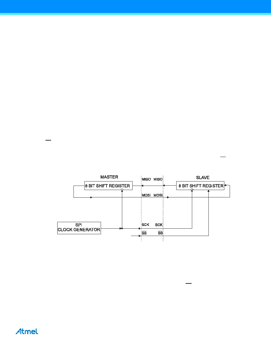
interconnection between master and slave devices with SPI is shown in Figure 20-1 on page 225. The system consists of
two shift registers and a master clock generator. The SPI master initiates the communication cycle by pulling the slave
select (SS) signal low for the desired slave. Master and slave prepare the data to be sent in their respective shift
registers, and the master generates the required clock pulses on the SCK line to interchange data. Data are always
shifted from master to slave on the master output, slave input (MOSI) line, and from slave to master on the master input,
slave output (MISO) line. After each data packet, the master can synchronize the slave by pulling the SS line high.
Figure 20-1. SPI master-slave interconnection.
The SPI module is unbuffered in the transmit direction and single buffered in the receive direction. This means that bytes
to be transmitted cannot be written to the SPI DATA register before the entire shift cycle is completed. When receiving
data, a received character must be read from the DATA register before the next character has been completely shifted in.
Otherwise, the first byte will be lost.
In SPI slave mode, the control logic will sample the incoming signal on the SCK pin. To ensure correct sampling of this
clock signal, the minimum low and high periods must each be longer than two CPU clock cycles.
When the SPI module is enabled, the data direction of the MOSI, MISO, SCK, and SS pins is overridden according to
Table 20-1 on page 226. The pins with user-defined direction must be configured from software to have the correct
direction according to the application.
SHIFT
ENABLE
msb
lsb
msb
lsb
发布紧急采购,3分钟左右您将得到回复。
相关PDF资料
PIC18F4321T-I/ML
IC PIC MCU FLASH 4KX16 44QFN
PIC18F4221T-I/ML
IC PIC MCU FLASH 2KX16 44QFN
PIC18F2321T-I/ML
IC PIC MCU FLASH 4KX16 28QFN
PIC18F2221T-I/SO
IC PIC MCU FLASH 2KX16 28SOIC
PIC16LF1939-I/MV
IC MCU 8BIT 28KB FLASH 40-UQFN
PIC24F16KL402-I/SP
IC MCU 16BIT 16KB FLASH 28-SPDIP
PIC18F24J11-I/SS
IC PIC MCU FLASH 16K 2V 28-SSOP
PIC24F16KA101-I/SO
IC PIC MCU FLASH 16K 20-SOIC
相关代理商/技术参数
PIC18F4450T-I/PT
功能描述:8位微控制器 -MCU 16KB FL 768 RAM 34 I/O FS-USB 2.0 RoHS:否 制造商:Silicon Labs 核心:8051 处理器系列:C8051F39x 数据总线宽度:8 bit 最大时钟频率:50 MHz 程序存储器大小:16 KB 数据 RAM 大小:1 KB 片上 ADC:Yes 工作电源电压:1.8 V to 3.6 V 工作温度范围:- 40 C to + 105 C 封装 / 箱体:QFN-20 安装风格:SMD/SMT
PIC18F4455-BL
制造商:POWERLITE SYSTEMS 功能描述:PIC18F445 W/ BOOTLOADER FOR FLASHLAB 制造商:POWERLITE SYSTEMS 功能描述:PIC18F445 W/ BOOTLOADER, FOR FLASHLAB 制造商:POWERLITE SYSTEMS 功能描述:PIC18F445 W/ BOOTLOADER, FOR FLASHLAB; Silicon Manufacturer:Powerlite Systems; Core Architecture:PIC; Kit Contents:Board; Features:Bootloader Programming, RS232 Connector for Boot-Loading and Serial Comms ;RoHS Compliant: Yes
PIC18F4455-I/ML
功能描述:8位微控制器 -MCU 24kBF 2048RM FSUSB2 RoHS:否 制造商:Silicon Labs 核心:8051 处理器系列:C8051F39x 数据总线宽度:8 bit 最大时钟频率:50 MHz 程序存储器大小:16 KB 数据 RAM 大小:1 KB 片上 ADC:Yes 工作电源电压:1.8 V to 3.6 V 工作温度范围:- 40 C to + 105 C 封装 / 箱体:QFN-20 安装风格:SMD/SMT
PIC18F4455-I/P
功能描述:8位微控制器 -MCU 24kBF 2048RM FSUSB2 RoHS:否 制造商:Silicon Labs 核心:8051 处理器系列:C8051F39x 数据总线宽度:8 bit 最大时钟频率:50 MHz 程序存储器大小:16 KB 数据 RAM 大小:1 KB 片上 ADC:Yes 工作电源电压:1.8 V to 3.6 V 工作温度范围:- 40 C to + 105 C 封装 / 箱体:QFN-20 安装风格:SMD/SMT
PIC18F4455-I/PT
功能描述:8位微控制器 -MCU 24kBF 2048RM FSUSB2 RoHS:否 制造商:Silicon Labs 核心:8051 处理器系列:C8051F39x 数据总线宽度:8 bit 最大时钟频率:50 MHz 程序存储器大小:16 KB 数据 RAM 大小:1 KB 片上 ADC:Yes 工作电源电压:1.8 V to 3.6 V 工作温度范围:- 40 C to + 105 C 封装 / 箱体:QFN-20 安装风格:SMD/SMT
PIC18F4455T-I/ML
功能描述:8位微控制器 -MCU 24kBF 2048RM FSUSB2 RoHS:否 制造商:Silicon Labs 核心:8051 处理器系列:C8051F39x 数据总线宽度:8 bit 最大时钟频率:50 MHz 程序存储器大小:16 KB 数据 RAM 大小:1 KB 片上 ADC:Yes 工作电源电压:1.8 V to 3.6 V 工作温度范围:- 40 C to + 105 C 封装 / 箱体:QFN-20 安装风格:SMD/SMT
PIC18F4455T-I/PT
功能描述:8位微控制器 -MCU 24kBF 2048RM FSUSB2 RoHS:否 制造商:Silicon Labs 核心:8051 处理器系列:C8051F39x 数据总线宽度:8 bit 最大时钟频率:50 MHz 程序存储器大小:16 KB 数据 RAM 大小:1 KB 片上 ADC:Yes 工作电源电压:1.8 V to 3.6 V 工作温度范围:- 40 C to + 105 C 封装 / 箱体:QFN-20 安装风格:SMD/SMT
PIC18F4458-I/ML
功能描述:8位微控制器 -MCU 24KB Flash 2KB RAM RoHS:否 制造商:Silicon Labs 核心:8051 处理器系列:C8051F39x 数据总线宽度:8 bit 最大时钟频率:50 MHz 程序存储器大小:16 KB 数据 RAM 大小:1 KB 片上 ADC:Yes 工作电源电压:1.8 V to 3.6 V 工作温度范围:- 40 C to + 105 C 封装 / 箱体:QFN-20 安装风格:SMD/SMT